
|
Hitech Circuits Co.,Limited
|


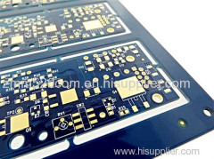
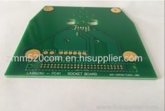
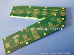
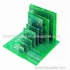
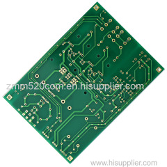
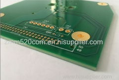
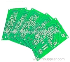
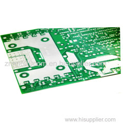
Multilayer PCB Circuit Boards
| Price: | 2.35 USD |
| Payment Terms: | T/T,L/C,D/A,D/P,WU,Paypal,Money Gram |
| Place of Origin: | Guangdong, China (Mainland) |
|
|
|
| Add to My Favorites | |
| HiSupplier Escrow |
Product Detail
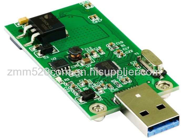
Printed Circuit Board can be found a self-contained module of interconnected electronic components found in all even the simplest electronic devices.
Multilayer PCB Circuit Boards Manufactur in Shenzhen

1>Our Superiority is the Professionalism of our team.
- PCB And PCB Assembly For One-stop Service with Original Components According the BOM.
IC Imported from Digikey / Farnell etc.
- Low Cost with High Quality, Commitment of Quality Assurance.
- For 10 years Experience in PCB Field. ( Our Factory owns advanced
production equipment and experienced technical personnel. )
2> Detailed specification of manufaturing capacity:
NO | Item | Craft Capacity |
1 | Layer | 1-30 Layers |
2 | Base Material for PCB | FR4, CEM-1, TACONIC, Aluminium, High Tg Material, High Frequence ROGERS ,TEFLON, ARLON, Halogen-free Material |
3 | Rang of finish baords Thickness | 0.21-7.0mm |
4 | Max size of finish board | 900MM*900MM |
5 | Minimum Linewidth | 3mil (0.075mm) |
6 | Minimum Line space | 3mil (0.075mm) |
7 | Min space between pad to pad | 3mil (0.075mm) |
8 | Minimum hole diameter | 0.10 mm |
9 | Min bonding pad diameter | 10mil |
10 | Max proportion of drilling hole and board thickness | 1:12.5 |
11 | Minimum linewidth of Idents | 4mil |
12 | Min Height of Idents | 25mil |
13 | Finishing Treatment | HASL (Tin-Lead Free), ENIG(Immersion Gold), Immersion Silver , Gold Plating (Flash Gold), OSP, etc. |
14 | Soldermask | Green, White, Red, Yellow, Black, Blue, transparent photosensitive soldermask, Strippable soldermask. |
15 | Minimun thickness of soldermask | 10um |
16 | Color of silk-screen | White, Black, Yellow ect. |
17 | E-Testing | 100% E-Testing (High Voltage Testing); Flying Probe Testing |
18 | Other test | ImpedanceTesting,Resistance Testing, Microsection etc., |
19 | Date file format | GERBER FILE and DRILLING FILE, PROTEL SERIES, PADS2000 SERIES, Powerpcb SERIES, ODB++ |
20 | Special technological requirement | Blind & Buried Vias and High Thickness copper |
21 | Thickness of Copper | 0.5-14oz (18-490um) |
3> Quote Requirements for PCB and PCB Assembly project:
- Gerber File and Bom List;
- Quote Quantity;
- Advise your technical requirements for quoting reference;
- Clearly picturers of PCB or PCB Assembly Sample to us for reference;
- Test Mothod for PCB Assembly.
4> Equipment List
NO. | Machine Name | QTY | NO. | Machine Name | QTY |
1 | PRESS | 2 | 10 | Exposurer | 5 |
2 | X-Ray | 1 | 11 | Deveoloper | 3 |
3 | Brown-Oxidation | 1 | 12 | Auto V-cut | 1 |
4 | Drilling | 13 | 13 | AOI | 2 |
5 | Cutter | 1 | 14 | Routing | 7 |
6 | PTH | 1 | 15 | ETS | 12 |
7 | PAL | 1 | 16 | Fly Probe | 4 |
8 | PAT | 1 | 17 | YAMAHA SMT | 3 |
9 | Flash Gold | 1 | 18 | FUJI SMT | 4 |
5> PCB and PCB Assembly Lead time:
Description | Double side | Four Layers | Six Layers | Above Eight | HDI |
Sample | 4 | 7 | 9 | 9 | 12 |
Mass production | 7-9 | 10-12 | 13-15 | 16 | 20 |
Assembly | 7-9 | 15 | 16 | 18 | 25 |
6> T-SOAR can be trusted PCB Partner, We are waiting for cooperation with you anytime.
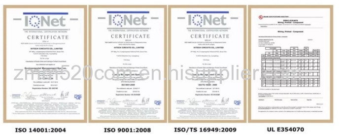
- UL, RoHS, ISO, SGS Certification Compliance.
- OEM Assembly, Design, Prototype Service.
- We will be responsible for the quality of our products,
- Survive by quality, Win by Price.
RFQ
Q1:What service do you have?
IBE: We provide turnkey solution including RD, PCB fabrication, SMT, plastic injection & metal, final assembly,testing and other value-added service.
Q2:What are the main products of your PCB/PCBA services?
IBE: Our PCB/PCBA services are mainly for the industries including Medical, Automotive, Energy, Metering/Measurements, Consumer Electronics.
Q3:Is IBE a factory or trade company?
IBE: IBE is a factory with PCB factory located in China and SMT assembly factories in both China & USA.
Q4:Can we inspect quality during production?
IBE: Yes, we are open and transparent on each production process with nothing to hide. We welcome customer inspect our production process and check in house.
Q5:How can we ensure our information should not let third party to see our design?
IBE: We are willing to sign NDA effect by customer side local law and promising to keep customers data in high confidential level.
Q6:What files required to get quotation from you?
IBE: For PCB quotation, please provide the Gerber data/files and indication of related technical requirements as well as any special requirement if you have.
For PCBA quotation, please provide Gerber data/ files and also BOM (bill of materials), and if you need us to do function test, please also provide the test instruction/procedure.
Q7:What is standard delivery term?
IBE: Delivery terms of EXW, FCA, FOB, DDU etc. are all available based on each quote.
Q8:How long does it take for PCB quote?
IBE: Normally 24 hours to 48 hours as soon as receive internal engineer evaluate confirmation.
Q9:Do you have any minimum order quantity (MOQ) requirement?
IBE: No, we do not have MOQ requirement, we can support your projects starting from prototypes to mass productions.
Email: sales10(at)hitechcircuits(dot)com
Didn't find what you're looking for?
Post Buying Lead or contact
HiSupplier Customer Service Center
for help!
Related Search
Pcb Circuit Boards
Multilayer PCB
20 Multilayer Pcb
Multilayer Printed Circuit Board
Prototype Printed Circuit Boards
Printed Circuit Boards
More>>
Find more related products in following catalogs on Hisupplier.com
Company Info
Hitech Circuits Co.,Limited [China (Mainland)]
Business Type:Manufacturer
City: Shenzhen
Province/State: Guangdong
Country/Region: China (Mainland)
|
zero:
|
You May Like:
Product (26)
- pcba (4)
- ceramic pcb (1)
- aluminum pcb (4)
- flex-rigid pcb (5)
- flex pcb (2)
- rigid pcb (10)
