
|
Hitech Circuits Co.,Limited
|
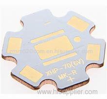


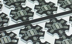
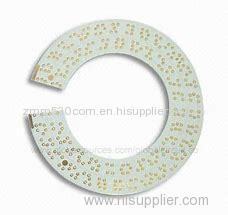
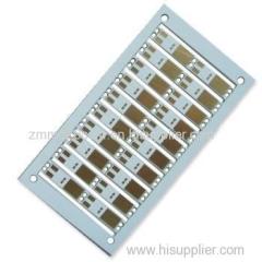
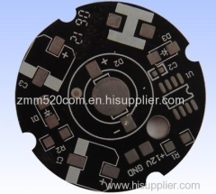
Multi-Function Manufacturer Large Quantity Copper Base Aluminum Base PCB Board
| Price: | 2.35 USD |
| Payment Terms: | T/T,D/A,D/P,WU,Paypal,Money Gram |
| Place of Origin: | Guangdong, China (Mainland) |
|
|
|
| Add to My Favorites | |
| HiSupplier Escrow |
Product Detail
Printed Circuit Board can be found a self-contained module of interconnected electronic components found in all even the simplest electronic devices.
Multi-Function Manufacturer Large Quantity Copper Base Aluminum Base PCB Board


Why us?
1.We are PCB & PCB assembly manufacturer with 12 years experience
2.UL&Rohs&ISO9001 certificated
3.4 times 100% QC inspection before Shipping.
4. Profeesional one-stop service release your energy to focus on design and marketing.
5.First order delivery time is around 15days, next order we will produce enough goods in stock for long cooperation.
6.Sign NDA to keep your design safe.
Our Service:
1. We will reply for you within 24hours once we get your inquiry.
2.Produce almost any LED pcb as your requirement.
3.We can offer you unique design and some our current models.
4.100%testing guarrantees stable quality, ISO 9001:2000 ,UL, RoHS certification

Lead Time:
| Lead time for sample | 2~3days for single-side board |
| 4~5days for double-side board | |
| 24~48hours for ugent | |
| Lead time for opening mould | 3~5days for normal mould |
| 5~7days for hard mould | |
| Lead time for mass production | 5~7days for single/double board |
Detailed specification of manufaturing capacity:
| NO | Item | Craft Capacity |
| 1 | Layer | 1-30 Layers |
| 2 | Base Material for PCB | FR4, CEM-1, TACONIC, Aluminium, High Tg Material, High Frequence ROGERS ,TEFLON, ARLON, Halogen-free Material |
| 3 | Rang of finish baords Thickness | 0.21-7.0mm |
| 4 | Max size of finish board | 900MM*900MM |
| 5 | Minimum Linewidth | 3mil (0.075mm) |
| 6 | Minimum Line space | 3mil (0.075mm) |
| 7 | Min space between pad to pad | 3mil (0.075mm) |
| 8 | Minimum hole diameter | 0.10 mm |
| 9 | Min bonding pad diameter | 10mil |
| 10 | Max proportion of drilling hole and board thickness | 1:12.5 |
| 11 | Minimum linewidth of Idents | 4mil |
| 12 | Min Height of Idents | 25mil |
| 13 | Finishing Treatment | HASL (Tin-Lead Free), ENIG(Immersion Gold), Immersion Silver , Gold Plating (Flash Gold), OSP, etc. |
| 14 | Soldermask | Green, White, Red, Yellow, Black, Blue, transparent photosensitive soldermask, Strippable soldermask. |
| 15 | Minimun thickness of soldermask | 10um |
| 16 | Color of silk-screen | White, Black, Yellow ect. |
| 17 | E-Testing | 100% E-Testing (High Voltage Testing); Flying Probe Testing |
| 18 | Other test | ImpedanceTesting,Resistance Testing, Microsection etc., |
| 19 | Date file format | GERBER FILE and DRILLING FILE, PROTEL SERIES, PADS2000 SERIES, Powerpcb SERIES, ODB++ |
| 20 | Special technological requirement | Blind & Buried Vias and High Thickness copper |
| 21 | Thickness of Copper | 0.5-14oz (18-490um) |
Company Information:
China pcb manufacturer--Hitech Circuits Co.,Limited, founded in 1997 in Shenzhen, adjoining to Hong Kong with easy transportation and ideal location. At the beginning we are a PCB distributor, since our formation, we have been strongly focusing on quality, cost, and service, and experienced continuous growth.
In order to give our customers a better service and be more competitive in the PCB market, we had stepped into the PCB manufacturing area in 2002 by share holding and controlling of two qualified PCB manufacturers. Now Hitechs facility total area is 65,000 square meters and have around 1600 experienced workers try our best to ensure the board quality and on time delivery.
Hitech focuses on high-mix, low volume and quick turn pcb service. With a special market position and excellent corporate culture, we can provide "One-stop shop" service from 1 to 26 layers of PCB products, which includs double layers PCB, Multilayer PCB, Aluminium PCB (Metal core PCB) Flexible PCB (FPCB), Rigid-Flex PCB (Flex-rigid PCB), High Density Interconnect (HDI )PCB boards, heavy copper boards, buried Capacitance & resistance boards, etc. Our products cover various products are exported to Europe, America and Asia.

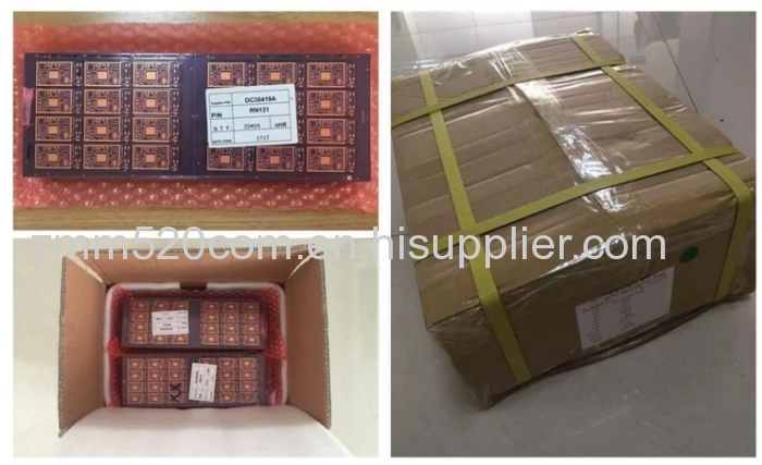
Packaging Details
1.Firstly seal products with hermetic plastic bag vrey well
2.Then using bubble or foam sheet to seperate them
3.Finally paper carton packing
Quotation requirements for PCB and PCB Asssembly project:
- Gerber File and Bom List;
- Quote Quantity;
- Advise your technical requirements for quoting reference;
- Clearly picturers of PCB or PCB Assembly Sample to us for reference;
- Test Mothod for PCB Assembly.
Related Search
Base Pcb
Aluminum Base
Copper Base Metal
Wall Base Board
Aluminum Casting Base
Heavy Copper Board Pcb
More>>
Find more related products in following catalogs on Hisupplier.com
Company Info
Hitech Circuits Co.,Limited [China (Mainland)]
Business Type:Manufacturer
City: Shenzhen
Province/State: Guangdong
Country/Region: China (Mainland)
|
zero:
|
You May Like:

Product (26)
- pcba (4)
- ceramic pcb (1)
- aluminum pcb (4)
- flex-rigid pcb (5)
- flex pcb (2)
- rigid pcb (10)
