
|
Hitech Circuits Co.,Limited
|


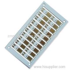
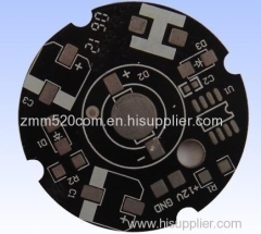
custom mcpcb/aluminium pcb board prototyping for led and led light circuit board in china
| Price: | 2.35 USD |
| Payment Terms: | T/T,L/C,D/P,WU,Paypal,Money Gram |
| Place of Origin: | Guangdong, China (Mainland) |
|
|
|
| Add to My Favorites | |
| HiSupplier Escrow |
Product Detail
Printed Circuit Board can be found a self-contained module of interconnected electronic components found in all even the simplest electronic devices.
custom mcpcb/aluminium pcb board prototyping for led and led light circuit board in china


About the Aluminum PCB
Aluminum PCB is one of metalbased pcb,including copper foil,thermal insulating layer and metal substrate,its structure divide into three layers:
1. Circuit layer: the equivalent of an ordinary PCB,copper thickness from 1oz to 10oz.
2. Insulation layer: Insulation is a layer of thermal insulating material with low thermal resistance.Thickness: 0.003 "to 0.006" inch is the aluminum pcb core technology.
3. Based Layer: a metal substrate,usually aluminum or copper may be chosen.
Our Superiority is the Professionalism of our team.
- PCB And PCB Assembly For One-stop Service with Original Components According the BOM.
IC Imported from Digikey / Farnell etc.
- Low Cost with High Quality, Commitment of Quality Assurance.
- For 10 years Experience in PCB Field. ( Our Factory owns advanced
production equipment and experienced technical personnel. )
PCB and PCB Assembly Lead time:
| Description | Double side | Four Layers | Six Layers | Above Eight Layers | HDI |
| Sample | 4 | 7 | 9 | 9 | 12 |
| Mass production | 7-9 | 10-12 | 13-15 | 16 | 20 |
| Assembly | 7-9 | 15 | 16 | 18 | 25 |
T-SOAR can be trusted PCB Partner, We are waiting for cooperation with you anytime.
- UL, RoHS, ISO, SGS Certification Compliance.
- OEM Assembly, Design, Prototype Service.
- We will be responsible for the quality of our products,
- Survive by quality, Win by Price.
Detailed specification of manufaturing capacity:
| NO | Item | Craft Capacity |
| 1 | Layer | 1-30 Layers |
| 2 | Base Material for PCB | FR4, CEM-1, TACONIC, Aluminium, High Tg Material, High Frequence ROGERS ,TEFLON, ARLON, Halogen-free Material |
| 3 | Rang of finish baords Thickness | 0.21-7.0mm |
| 4 | Max size of finish board | 900MM*900MM |
| 5 | Minimum Linewidth | 3mil (0.075mm) |
| 6 | Minimum Line space | 3mil (0.075mm) |
| 7 | Min space between pad to pad | 3mil (0.075mm) |
| 8 | Minimum hole diameter | 0.10 mm |
| 9 | Min bonding pad diameter | 10mil |
| 10 | Max proportion of drilling hole and board thickness | 1:12.5 |
| 11 | Minimum linewidth of Idents | 4mil |
| 12 | Min Height of Idents | 25mil |
| 13 | Finishing Treatment | HASL (Tin-Lead Free), ENIG(Immersion Gold), Immersion Silver , Gold Plating (Flash Gold), OSP, etc. |
| 14 | Soldermask | Green, White, Red, Yellow, Black, Blue, transparent photosensitive soldermask, Strippable soldermask. |
| 15 | Minimun thickness of soldermask | 10um |
| 16 | Color of silk-screen | White, Black, Yellow ect. |
| 17 | E-Testing | 100% E-Testing (High Voltage Testing); Flying Probe Testing |
| 18 | Other test | ImpedanceTesting,Resistance Testing, Microsection etc., |
| 19 | Date file format | GERBER FILE and DRILLING FILE, PROTEL SERIES, PADS2000 SERIES, Powerpcb SERIES, ODB++ |
| 20 | Special technological requirement | Blind & Buried Vias and High Thickness copper |
| 21 | Thickness of Copper | 0.5-14oz (18-490um) |
Quote Requirements for PCB and PCB Assembly project
- Gerber File and Bom List;
- Quote Quantity;
- Advise your technical requirements for quoting reference;
- Clearly picturers of PCB or PCB Assembly Sample to us for reference;
- Test Mothod for PCB Assembly.
Related Search
Find more related products in following catalogs on Hisupplier.com
Company Info
Hitech Circuits Co.,Limited [China (Mainland)]
Business Type:Manufacturer
City: Shenzhen
Province/State: Guangdong
Country/Region: China (Mainland)
|
zero:
|
You May Like:

Product (26)
- pcba (4)
- ceramic pcb (1)
- aluminum pcb (4)
- flex-rigid pcb (5)
- flex pcb (2)
- rigid pcb (10)
